Read next
CATDOLL 126CM Yoyo
Height: 126cm Weight: 23kg Shoulder Width: 32cm Bust/Waist/Hip: 61/58/66cm Oral Depth: 3-5cm Vaginal Depth: 3-15cm Anal...
Articles
2026-02-22
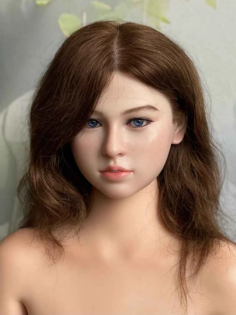
CATDOLL 148CM Christina Silicone Doll
Articles
2026-02-22
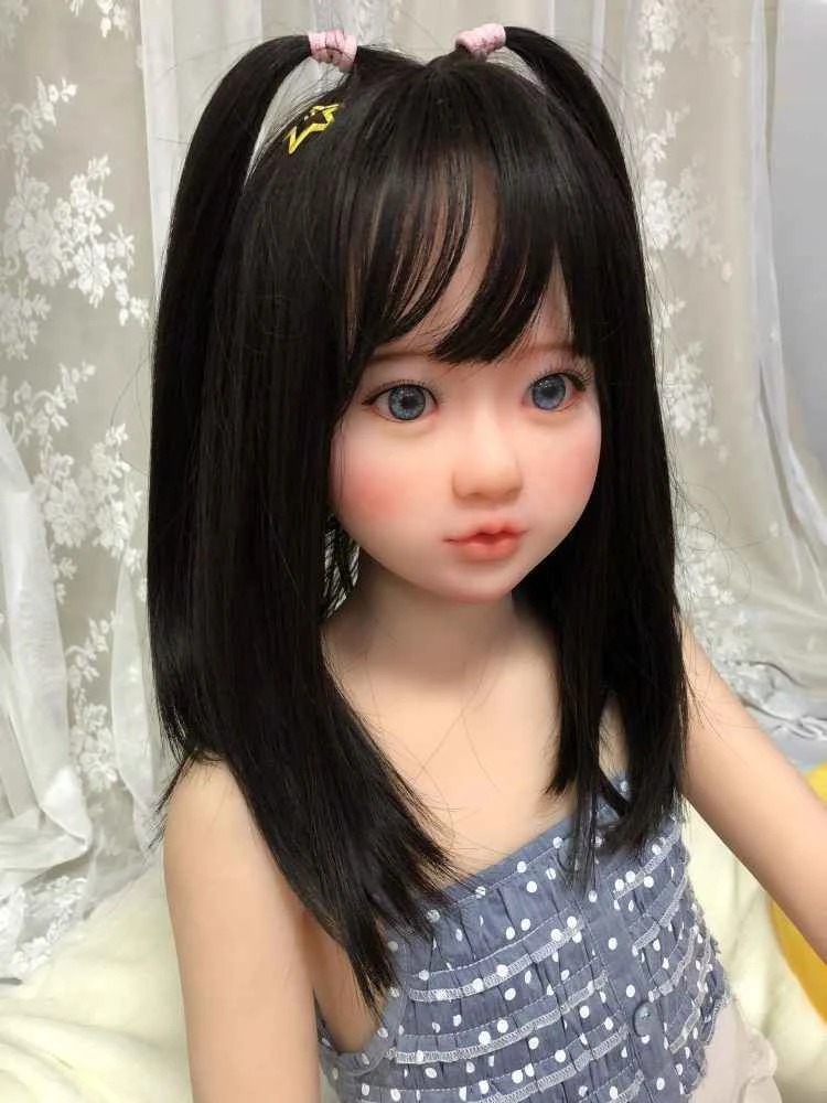
CATDOLL 128CM Emelie Open Eyes Type
Articles
2026-02-22
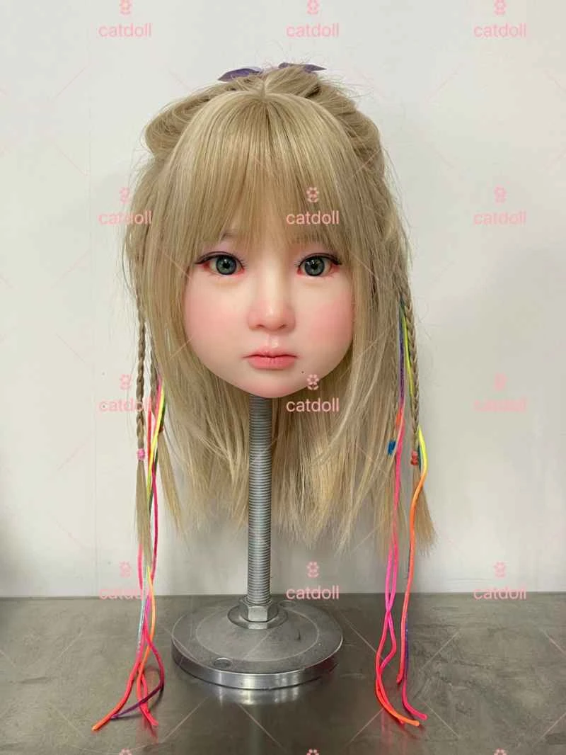
CATDOLL Dudu Soft Silicone Head
Articles
2026-02-22