Read next
Precautions for the installation and maintenance of programmable logic controllers
Programmable Logic Controllers (PLCs) are a new type of general-purpose automation control device that integrates tradit...
Articles
2026-02-22
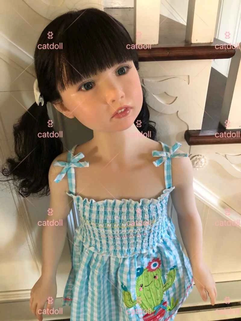
CATDOLL 108CM Coco Full Silicone Doll
Articles
2026-02-22
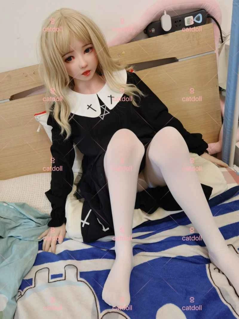
CATDOLL 126CM Yoyo (Customer Photos)
Articles
2026-02-22
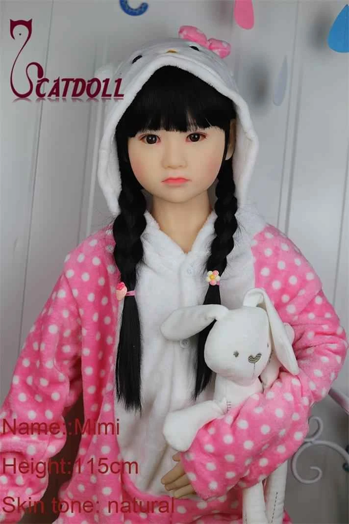
CATDOLL 115CM Mimi TPE
Articles
2026-02-22