Read next
CATDOLL Amber Hybrid Silicone Head
The hybrid silicone head is crafted using a soft silicone base combined with a reinforced scalp section, allowing durab...
Articles
2026-02-22
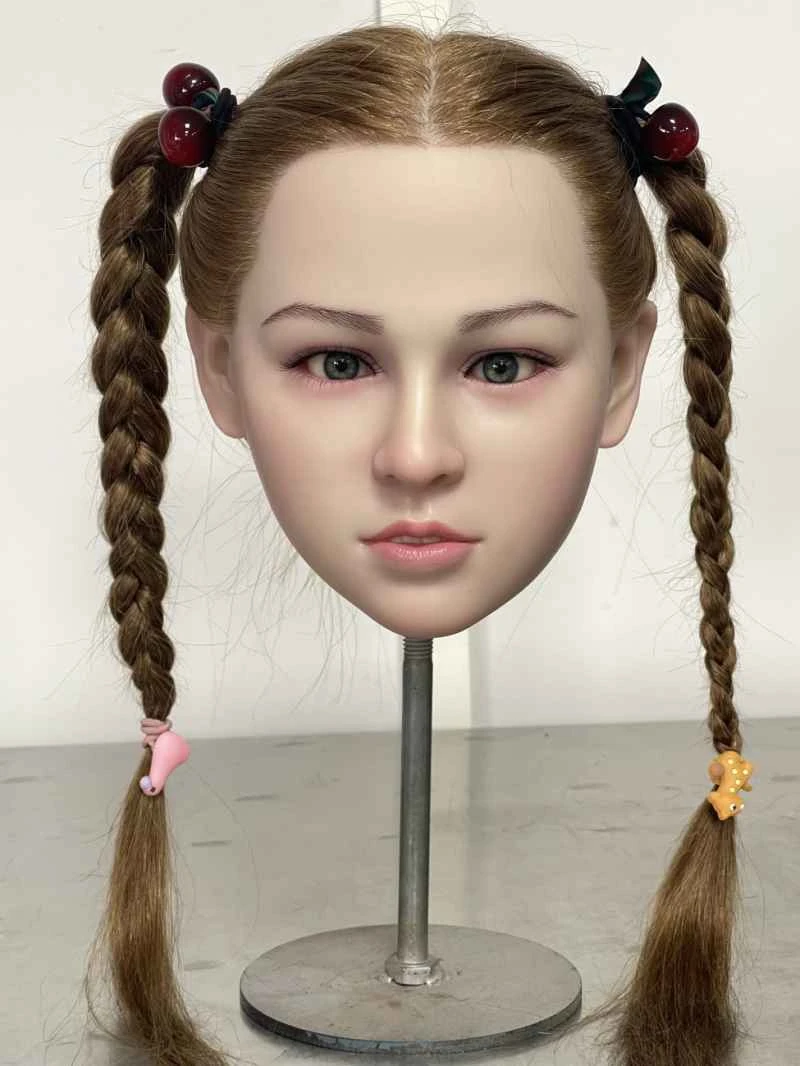
CATDOLL Christina Hard Silicone Head
Articles
2026-02-22
CATDOLL 108CM Dodo (TPE Body with Hard Silicone Head)
Articles
2026-02-22
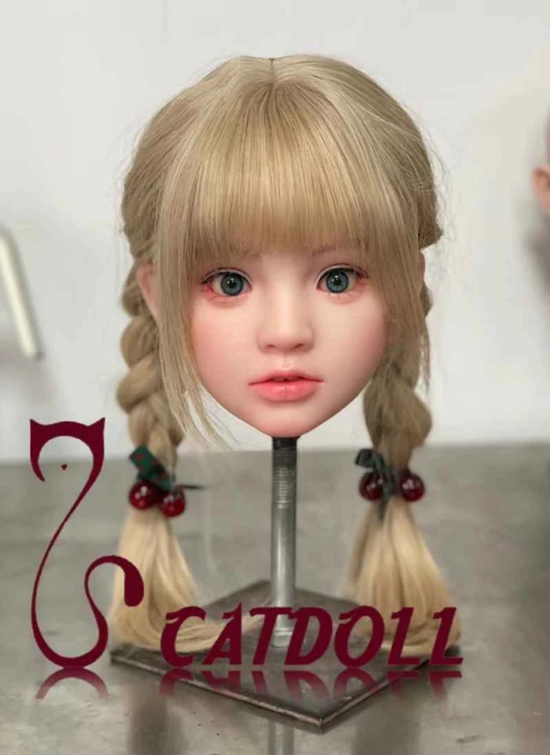
CATDOLL Milana Soft Silicone Head
Articles
2026-02-22