Read next
CATDOLL 101cm TPE Doll with Anime A-Type Head – Cute Petite Body
Height: 101cm Weight: 15.5kg Shoulder Width: 26cm Bust/Waist/Hip: 57/50/66cm Oral Depth: 3-5cm Vaginal Depth: 3-13cm An...
Articles
2026-02-22
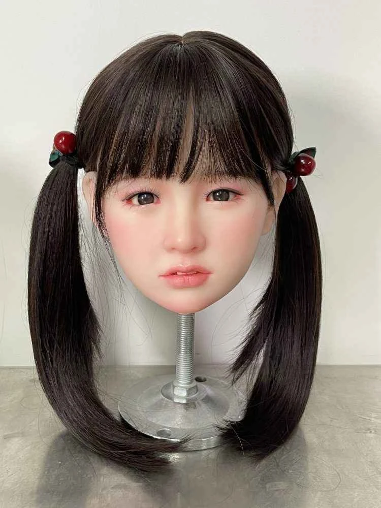
CATDOLL Chu Soft Silicone Head
Articles
2026-02-22
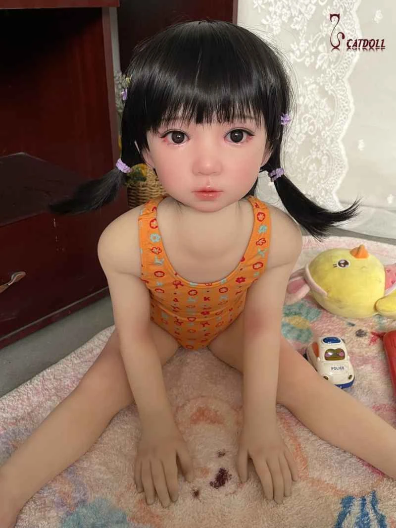
CATDOLL 88CM Maruko (soft Silicone Head with TPE Body)
Articles
2026-02-22
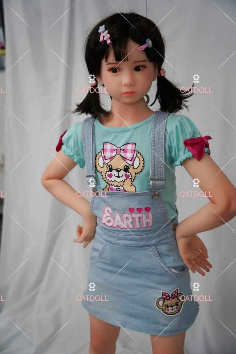
CATDOLL 130CM Kiki
Articles
2026-02-22