Read next
CATDOLL 146CM Sasha TPE
Height: 146cm A-cup Weight: 26kg Shoulder Width: 32cm Bust/Waist/Hip: 64/54/74cm Oral Depth: 3-5cm Vaginal Depth: 3-15c...
Articles
2026-02-22

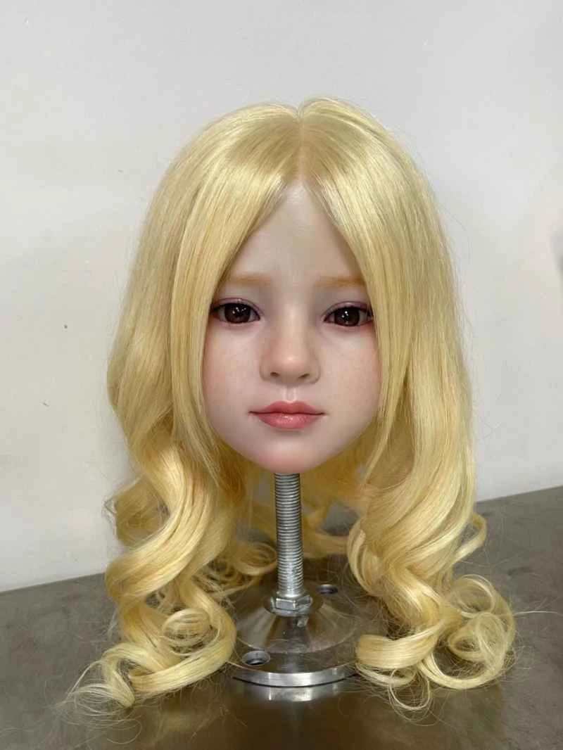
CATDOLL Ava Hard Silicone Head
Articles
2026-02-22

A Brief Discussion on Artistic Design in Human-Computer Interface Design
Articles
2026-02-22