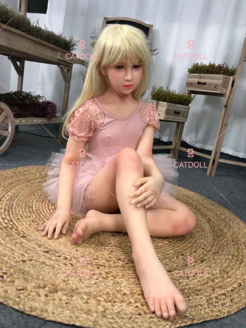
The impact of changes in the power unit structure of frequency converters on electromagnetic compatibility performance
2026-04-06 05:59:03··#1
1. Introduction In the topology of high-voltage, high-power frequency converters, the multi-level unit series voltage source frequency converter adopts a topology of multi-level superposition, standard low-voltage power unit structure in series, and internal capacitor array voltage regulation within the unit. Due to the characteristics of its topology, the system composition is complex with numerous internal components. However, the superposition characteristic of the topology allows for voltage and power upgrades simply by increasing the number and series configuration of standard low-voltage power units in the main topology, without requiring redesign of the power circuit components. Its versatility and inheritance advantages are very prominent, giving it a natural advantage in high-voltage and high-power applications. Therefore, multi-level unit series voltage source frequency converters are increasingly used in high-power, high-voltage environments. The performance and quality of the standard low-voltage power units are key to determining the performance of the multi-level unit series voltage source frequency converter. In practical applications, the standard low-voltage power units on a single phase in the power conversion circuit are developed from three in series, to six in series, and then to nine in series, enabling the output voltage level to range from 3kV to 6kV to 10kV. Although the voltage level and output power of each standard low-voltage power unit remain unchanged under different voltage levels, the electromagnetic operating environment of the power unit becomes increasingly harsh. With the increase in total voltage level and total output power, the spatial distribution of interference energy within each standard power unit increases, the non-periodic nature of its temporal distribution intensifies, the spectral bandwidth of the interference frequency increases, and the number of sources of interference increases accordingly. This deterioration of the electromagnetic compatibility environment severely affects the performance of the standard low-voltage power unit. Therefore, it is necessary to adopt corresponding electromagnetic compatibility technologies to ensure the power unit can operate stably through rigorous industrial electromagnetic environment testing, while maintaining its output characteristics, thereby guaranteeing the performance and quality of the multi-level unit series voltage source type high-voltage frequency converter system. 2. Basic Knowledge of Electromagnetic Compatibility The International Electrotechnical Commission (IEC) defines electromagnetic compatibility as: "Electromagnetic compatibility is the ability of a device to perform its functions in other environments without causing unacceptable interference in its own environment." China's national military standard GJB72-85 "Terminology of Electromagnetic Interference and Electromagnetic Compatibility" defines electromagnetic compatibility as: "A state of coexistence in which devices (subsystems, systems) can perform their respective functions together in a common electromagnetic environment, that is, the device will not suffer unacceptable performance degradation due to electromagnetic emissions from other devices in the same electromagnetic environment." 2.1 EMC Test Item - Introduction to Electrical Fast Transient Burst (EFT) (1) Sources of EFT Interference A common transient interference in electrical and electromechanical equipment, it is generated by inductive devices such as relays, motors, and transformers. Generally, these devices are part of the system, so the interference is often generated inside the system. (2) Effects of EFT on Equipment Electrical fast transient bursts are generated when an inductive load in a circuit is disconnected. Its characteristic is a series of pulses, so it has a significant impact on the circuit. A series of pulses in the circuit can have a cumulative effect at the circuit input, causing the amplitude of the interference level to eventually exceed the noise threshold of the circuit. From this mechanism, the shorter the period of the pulse train, the greater the impact on the circuit. Because when each pulse in the pulse train is very close, the circuit input capacitor does not have enough time to discharge before it starts charging again, which can easily reach a high level and extinguish the normal input signal. (3) Characteristics of EFT When the inductive load switching system is disconnected, transient interference (EFT) will be generated at the break point. This transient interference consists of a large number of pulses. Measurements on the 220V power line show that the amplitude of this pulse group is between 100V and several kilovolts. The specific size is determined by the electrical characteristics of the switch contacts (such as the speed of contact opening, the withstand voltage level when the contact is disconnected, the contact arc extinguishing mechanism, etc.). The pulse repetition frequency is between 1kHz and 1MHz. For a single pulse, its rising edge is in the nanosecond range, and the pulse duration is between tens of nanoseconds and several milliseconds. The spectrum distribution of this interference signal is very wide. High-speed digital circuits are more sensitive to it and are easily disturbed. From the actual test results, it was found that a large number of products (mainly digital devices) could not withstand this kind of interference, and often the phenomena of program chaos, data loss, and control circuit failure occurred. (4) EFT standard IEC has specially formulated the standard IEC61000-4-4 (1995) "Electrical Fast Transient and Burst Immunity Test" to simulate the impact of electrical fast transient and burst on electrical and electronic equipment. The corresponding national standard is GB/T13926.4-92 "Electromagnetic compatibility of industrial process measurement and control devices - requirements for electrical fast transient and burst". Because this standard has a great influence internationally, many international organizations or some domestic relevant departments have introduced this standard into their product standards or general standards. 2.2 Suppression methods of electrical fast transient and burst interference (1) Reduce the common impedance of PCB ground line At the IC input terminal, EFT charges the parasitic capacitance. Through the gradual accumulation of many pulses, it finally reaches and exceeds the immunity limit of IC. Since any ground wire has both resistance and reactance, a voltage drop will inevitably occur when current flows through it, which can easily generate a potential difference. This can be reduced by using good wiring and increasing the area of the grounding wire to make it lower than the anti-interference level of the digital circuit. (2) Use EFT inductor transient interference suppression network to use EFT filters or absorbers to keep the interference source away from sensitive circuits; (3) Use grounding technology correctly; (4) Add anti-interference instructions in the software; (5) Install transient interference absorbers. Usually, the above methods are combined according to the specific situation to achieve the best effect. 3 Introduction to the electromagnetic compatibility test platform and the goal of electromagnetic compatibility improvement of power unit3.1 Electromagnetic compatibility performance test platform of power unit Location: Electromagnetic compatibility laboratory of Harbin Institute of Technology. Instrument: EMC TRANSIENT 2000. Test object: Prototype of inverter power unit Executor: R&D staff of Harbin Jiuzhou Electric Co., Ltd.: Li Kai, Bai Defang Doctoral candidate of Department of Electrical Engineering of Harbin Institute of Technology: Yan Dong Power unit structure modification site: Laboratory of Development Center of Harbin Jiuzhou Electric Co., Ltd. 3.2 Target for Improving the Electromagnetic Performance of the Power Unit The power unit will pass the severe industrial environment level of 4.0kV, 2.5kHz, 30s EMF/BRT test. After the power unit's EMF is completed, the external connection space will remain unchanged, and it can be directly installed in the original cabinet. The structural modifications to the power unit will focus on the external structure, without changing the relative positions of the internal components. The cost of improving EMF will be controlled within 10% of the total cost of the power unit. The operating mode of the internal power components in the modified power unit will remain unchanged. The completion time for the research on improving the EMF of the power unit is scheduled for three months. 3.3 Prototype Power Unit with Improved EMF Performance The standard power unit with a capacity of 600V-63A will be modified to meet the highest severe industrial environment level required to pass EMF testing. The prototype structure before modification is shown in Figure 1. [align=center] Figure 1 Power unit prototype structure diagram[/align] 4 Conduct electromagnetic compatibility performance tests on the power unit prototype and analyze the key points of weak electromagnetic performance4.1 Conduct electromagnetic compatibility tests on the power unit prototype (1) Pre-test plan The premise for conducting electromagnetic compatibility performance analysis on the power unit prototype of the multi-level unit series voltage source inverter is to conduct rigorous electromagnetic compatibility tests on it. In the electromagnetic compatibility laboratory of Harbin Institute of Technology, the power unit prototype is tested in a multi-level, multi-time, and multi-verification manner. The highest test standard is set at the level standard of harsh industrial environment. (2) After the test, the data after the test is completed is summarized in Table 1. Table 1 Data summary after the test 4.2 Based on the test results, conduct in-depth analysis of the electromagnetic compatibility performance of the power unit (1) Electromagnetic compatibility performance level of the power unit The EMC performance of the multi-level power unit passed the level 3 test of electrical fast transient pulse group, but failed the level 4 test. That is, the current power unit's electrical fast pulse anti-interference characteristics have reached level 3, but have not yet reached level 4, that is, the standard for normal operation under harsh industrial environment. (2) When the power unit is tested by EFT, the key point of abnormal operation caused by EFT is that when the power unit is only powered on and in standby state, when a 4.0kV electrical fast transient burst is applied to it, all the status indicator lights on the power unit start to flash randomly and rapidly. Its EMI noise interference has completely disrupted the normal operation of the digital signal circuit. In the electrical fast transient burst test at 3.0kV and 2.5kHz, the power unit operates normally. When the test frequency is increased to 5kHz, it passes three times and fails twice in five tests with a length of 300s. This shows that 3.0kV is a critical value for the power unit's anti-interference capability against electrical fast transient bursts. 5. Based on the test results, conduct in-depth analysis and formulate the direction of the project based on the analysis results.5.1 In-depth analysis of the key points of faults that occur in electromagnetic compatibility testing (1) Analysis of the causes of intermittent faults When the test is conducted at 3.0kV, it operates normally at a frequency of 2.5kHz, but intermittent faults occur at a frequency of 5.0kHz. The cause of this issue is analyzed as follows: After the EFT signal enters through the power line, all interference signals at 2.5kHz are filtered out at the IC signal port, and the power unit operates normally. When the pulse frequency of the EFT interference increases to 5.0kHz, some of the interference signal will pass through the input filter and enter the subsequent circuit, charging the parasitic capacitance. Through the gradual accumulation of numerous pulses, this eventually reaches and exceeds the IC's immunity limit, causing the digital circuit to malfunction through direct triggering or electrostatic coupling. The accumulation of interference in the capacitor is affected by the IC circuit's operating state and the input filtering effect, resulting in a discrete fault, consistent with the fault occurrence patterns in the test data summary table. (2) Analysis of the cause of failure before operation When the power unit is powered on and in the stop state, a 4.0kV fast transient pulse group level interference is applied to it. All indicator lights are flashing, indicating that the interference level in the IC circuit has exceeded the noise threshold of the circuit. The noise in the digital circuit has annihilated the normal operating signal. It should not be caused by the cumulative effect of the pulse. It should be that the capacitive coupling or inductive coupling in the line is large. After the interference signal is input, the interference signal coupled out in the digital circuit directly exceeds the level of the normal operating signal in the circuit. When the power unit is in the stop state, a 4.0kV level interference is applied. Before it is even running, the indicator lights start to flash randomly. 5.2 Key points of unreasonable cable layout in the prototype of the power unit (1) The input main circuit cable and the control circuit cable are led from the input/output terminals at the front of the power unit to the rectifier diode and control transformer at the rear of the power unit. It is equivalent to all the input/output power first passing through the cable around half of the power unit before entering the corresponding components. (2) The 80V and 8V power cables of the main control board and the temperature alarm signal cable surround more than half of the space around the main control board. The voltage level difference between some long-distance parallel cables is large, the power supply types are many, the current density distribution is wide, and the mutual working spectrum area is complex. In general, the power and control cables are arranged in a ring in the unit, and they are long and have many parallel wirings. Due to the above cable layout, mutual interference is very likely to occur. At the same time, the long cable not only acts as an excellent antenna, but also has a large voltage difference during operation due to its long parallel length (the highest is 800V and the lowest is 5V), so its electromagnetic coupling phenomenon is relatively serious. 5.3 Combined with the analysis of test results and the specific power unit structure, the main reason for its weak electromagnetic compatibility performance is judged (1) Electromagnetic compatibility cable design In electromagnetic compatibility theory, the cable is a highly efficient electromagnetic wave receiving antenna. The electromagnetic interference in the space is often first received by the cable and then transmitted to the equipment, causing the digital circuit to malfunction. At the same time, the cable is also a very high electromagnetic wave radiation antenna. When the equipment is shielded, the cable is the main cause of electromagnetic wave radiation. When equipment or systems fail to meet the relevant electromagnetic interference limits, 90% of the time it is the cables that are the cause. (2) The direct factor that the power unit prototype failed the industrial-grade EFT test is that the cables in the power unit are not only numerous and messy, but also very long, which is almost like adding a large antenna network to the power unit. The analysis determined that the main reason for failing the Level 4 Electrical Fast Transient Burst Test should be that the cables are too long. 5.4 Target direction for improving the electromagnetic compatibility performance of the power unit prototype (1) The main object of the electromagnetic compatibility improvement of the power unit prototype Through the above analysis, the reason why the power unit fails the Level 4 Electrical Fast Transient Burst Test should be that the cables in the power unit are too long, too many are parallel, and cables of different voltage levels are mixed. The longest cable in the power unit is shown in Figure 2. The main object of the improvement of electromagnetic compatibility performance is these long cables. These long cables are shortened by structural modification, and the loop wiring method of the cables in the power unit is changed at the same time. [align=center] Figure 2 Long cable inside the power unit prototype[/align] (2) Direction of electromagnetic compatibility improvement of the power unit prototype Without changing the relative position of the main power components, change the shell form, output/input terminals, and fixed position of the main control board of the power unit prototype, thereby shortening and rearranging the long cable. 5.5 Feasibility direction of inverter power unit structure modification (1) According to the analysis of the power unit prototype structure, the general modification direction that can be achieved is that the original power supply wiring method of the power unit is to enter from the front of the power unit, pass through the long cable to the rectifier bridge and transformer at the rear of the power unit, and there is no connection with other electrical components during the wiring process. The long cable can be pulled out from the power unit, indicating that it is not connected to any component in the middle. The main cable is 1000mm long and the transformer cable is 700mm long. The existence of such a long cable is because the input rectifier is placed at the rear of the power unit, while the input line enters from the front. Adjusting the rectifier bridge of the power unit from the rear to the front can shorten the length of the input cable by about 2/3. Moving the input transformer from the rear to the front can shorten the cable from the transformer to the main control board power supply by about 2/3. (2) Analysis of the specific implementation method of the power unit structure modification according to the modification direction The shell of this power unit prototype is both the outer shell and the supporting frame of the internal components, as shown in Figure 2. It consists of three parts: the left side plate, the right side plate, and the main shell. In the specific structural installation, the power devices are fixed on the heat sink, the capacitors and their pre-charging devices are fixed on the right side plate, the main control board is fixed on the left side plate, and the input/output terminals are fixed on the front of the main shell. Taking advantage of the fact that the main shell only has input/output terminals, and all of them are cable connections, if the main shell of the power unit is flipped back and forth, the goal of moving the rectifier bridge and transformer from the rear to the front can be achieved without changing the relative position of the components inside. The modified internal hard connection copper strip can also continue to be used. 6. Formulate a preliminary structural modification plan for improving the electromagnetic compatibility performance of the inverter power unit.6.1 Methods for modifying the power unit structure (1) Changes in the installation and placement of the power unit: Mirror the main housing of the power unit from front to back, and mirror the installation position of the power unit from front to back. This changes the input rectifier bridge and control transformer of the power unit from the rear to the front. (2) Changes in the main housing of the power unit: After mirroring the main housing of the power unit, the corresponding horizontal output/input terminals do not need to be changed. The change is in the position of the main control board output port. The output interface of the main control board is reprocessed in the corresponding position. (3) Changes in the installation structure of the main control board: Rearrange the spatial position of the main control board according to the position of the output window on the modified power unit housing. When the main control board is still fixed on the left side plate, due to the change in spatial position, the components of the main control board will be hidden when the power unit is opened, which will cause great inconvenience to the factory testing and adjustment. In view of the above requirements, a bracket structure is made in the corresponding position in the power unit, and the main control board is installed on the bracket so that the component mounting surface of the main control board is on the outside, which is convenient for factory testing and inspection. 6.2 Determine the operational principles for structural modification of the power unit prototype for electromagnetic compatibility performance (1) Component usage principle: Use the original electrical components, keep the internal hard connection structure unchanged, and use changes to the soft connection structure and shell structure to achieve the goal of shortening the cable length. (2) Structural component usage principle: Use the original structure as much as possible when making the shell structure. If the original structure can be modified, use the original structure as much as possible and do not remake it, thereby accelerating the research and development process and speed. (3) Cable wiring principle: When making cables, strictly follow the technical requirements of electromagnetic compatibility to make cable wiring. The type of wire used and the wiring direction should be simple and not too complicated. Multi-layer wiring should be carried out according to the finished product type. (4) Power unit fixing principle: After the electromagnetic compatibility modification is completed, it can realize all the functions of the original power unit, and the spatial position of its output and input terminals cannot be changed. It can be directly installed into the original cabinet. All the structures and wiring in the cabinet do not need to be changed and are completely compatible with the installation type of the power unit prototype. (5) Process requirements during the research and development process. In the research and development process, under the premise of ensuring the above requirements, the appearance process that does not affect the electrical performance and test parameters can be relaxed appropriately to speed up the research and development. After the research and development of all electrical performance is completed, the detailed appearance structure treatment will be carried out. 6.3 Determination of structural components that are not modified in the power unit (1) Mounting components on the heat sink of the power unit The mounting structure of the components used on the heat sink remains unchanged and no changes are made. (2) Mounting structure of capacitor array The installation of capacitor array is changed from the right side plate to the left side plate as mirror of the power unit. Its relative position with the installation of all power devices on the heat sink remains unchanged. (3) Mounting structure of internal copper busbar In the structural change, the relative position of each device in the main circuit remains unchanged, that is, the internal copper busbar does not need to be changed and the original copper busbar structure can be directly used. 6.4 Structural components that need to be processed and manufactured (1) Main housing of the power unit A new main control board output window is processed on the right side of the main housing, and mounting holes for the main control board bracket are processed on the front and rear parts of the main housing. (2) The main control board bracket of the power unit is processed according to the installation position of the main control board. It is fixed on the corresponding mounting holes of the main housing. At the same time, the bracket also serves as a cable tray for internal cable layering. (3) The main control board shielding plate of the power unit is moved from the front side to the rear side of the main control board according to the installation position of the main control board. It is directly installed on the main control board bracket to ensure that the shielding structure of the main control board after the structure is completed maintains its original form. 7 Specific implementation steps of structural changes to improve the electromagnetic compatibility performance of the power unit of the frequency converter7.1 Parts whose installation position does not need to be changed (1) The installation of components on the radiator does not need to be changed. The original structure is maintained, as shown in Figure 3. [align=center] Figure 3 Heat sink installation structure[/align] (2) The capacitor array, voltage equalization plate, and transformer installation structure are not changed. The original right side is directly converted into the left side plate according to the predetermined plan. This method ensures that the internal copper busbar connection structure does not need to be changed and all power devices of the internal main power circuit can be installed. Only the outer shell, input/output leads, main control board and other parts that should be changed in the predetermined plan are not installed. The structure at this time is shown in Figure 4. [align=center] Figure 4 All structures that do not need to be changed[/align] 7.2 Change of the main shell structure of the power unit (1) When the main shell of the power unit prototype is mirrored back and forth, since the position of the rivet nut of the power unit of the prototype is arranged according to the longitudinal axis, after the position of the main shell is reversed back and forth, it can be installed on the left side plate. The main body is processed to make a main control board output window and bracket mounting hole. The main shell after installation is shown in Figure 5. [align=center][b] Figure 5 Main housing after processing[/b][/align] In Figure 6 after the main housing is assembled, it can be seen that according to the predetermined plan, after the main housing is interchanged front and back, the heat sink of the power unit is also interchanged front and back at the same time. Its input rectifier bridge and control transformer have been moved from the rear of the original power unit to the front of the power unit, and the length requirement of its wiring cable will be greatly reduced. [align=center] Figure 6 Main housing after assembly[/align] 7.3 Fabrication of main control board bracket in inverter power unit (1) Selection of main control board bracket material According to the relative spatial layout of the main control board in the power unit, the bracket should be between the positive electrode surface of the capacitor array and the predetermined spatial position of the main control board. In the stock materials, there are standard epoxy resin cast glass cloth layer insulating rods. They are directly used to make the bracket. Due to the insulating nature of its body, it has a very large margin of electrical clearance and insulation distance in the fabrication, and its processing is simple and easy. (2) Fabrication of the main control board bracket: First, cut two 30mm thick epoxy-cast glass cloth insulating rods into suitable lengths, drill holes at both ends, and tap internal threads for fixing with bolts above the mounting holes on the front and rear of the main housing. Drill equidistant standard holes longitudinally to serve as internal cable trays, and use the wiring rack for layered wiring of the wire harness as wire harness fixing holes. (3) Combining the main control board with the shielding layer: When designing the bracket, modify the shielding plate on the power unit prototype and fix it on the bracket. Used to shield the electromagnetic interference of the output copper plate of the capacitor array. After all the structural modifications to improve the electromagnetic compatibility performance are completed according to the predetermined plan, the main control board bracket is shown in Figure 7. [align=center] Figure 7 Main control board bracket after processing[/align] 7.4 Changes to inverter power unit wiring harness (1) Types of wiring harnesses IGBT drive wiring harness 4 sets Capacitor array soft start cut-off wiring harness 1 set Bypass control wiring harness 1 set Main control board power supply wiring harness 2 sets Capacitor array voltage measurement wiring harness 2 sets Temperature detection wiring harness 1 set IGBT output measurement wiring harness 1 set (2) Layered wiring harness design, as shown in Figure 8. [align=center] Figure 8 Layered wiring space structure of main control wiring harness[/align] Capacitor array voltage measurement and temperature detection are wired on the main control board bracket. Capacitor voltage divider measurement is wired on the main control board bracket. IGBT drive wiring harness is directly connected from IGBT to the main control board. Main control board power supply is wired in the front space between the control transformer and the bracket. Bypass control and soft start cut-off are wired on the surface of the heat sink. IGBT output measurement is wired at the rear of the power unit through the main control bracket fixing method. 7.5 Installation of the main control board of the inverter power unit and connection of all cables to complete the prototype (1) After fixing the main control board bracket on the casing of the inverter power unit, determine the length of the wire harness according to the spatial structure of the layered wire harness and the position of each terminal, and make its terminal. (2) Install the main control board on the bracket and connect the corresponding cables. The corresponding wire harness has been arranged. Install the main control board and connect the corresponding wire harness. At this time, the internal electrical structure of the power unit has been completely changed and is ready for power-on operation. After power-on, the operation status test can be carried out, as shown in Figure 9. [align=center] Figure 9 Main control board assembly diagram[/align] (3) Complete all structural changes and modifications of the power unit. After the installation of all electrical structures of the power unit is completed, assemble the right side plate, indicating that all structural changes are completed. The output and input terminals are consistent with the spatial position of the power unit prototype and have the performance of being directly installed in the inverter cabinet, indicating that the installation structure meets the requirements of the project. As shown in Figure 10: [align=center] Figure 10 Model after power unit structure modification[/align] 8 Electromagnetic compatibility performance test after power unit structure modification8.1 Load temperature rise and functional test After the power unit is modified, it is first powered on and tested with a power unit test box to verify whether it can work normally after the structure modification. After the operation and protection tests are passed, the temperature rise of each part is tested under full load. After 24 hours of full load test, the performance of the modified power unit fully meets the performance indicators of the power unit prototype. 8.2 Electromagnetic compatibility test (1) Electrical fast pulse group (EFT) test is conducted on the power unit in the electromagnetic compatibility laboratory of Harbin Institute of Technology. The test standard is carried out according to the highest severe industrial environment level, as shown in Figure 11. [align=center] Figure 11 Electromagnetic compatibility test after power unit structure modification[/align] (2) The test data after the structure modification is completed is summarized in Table 2. Table 2 Summary of test data after structural modification 8.3 Summary of electromagnetic compatibility test (1) The above data shows that the power unit after structural modification passed the highest level (level 4) of electrical fast transient burst (EFT) test, and its immunity to EFT has reached or even exceeded the standard for operation in harsh industrial environments. (2) After the power unit was structurally modified in accordance with EMC requirements, its EFT immunity level reached the target set by the project, indicating that the structural modification research and development task of improving the EMC performance of the power unit of the multi-level unit series voltage source inverter was successfully completed. 9 Determination of the reasons for poor electromagnetic compatibility performance of the power unit prototype9.1 The power unit before modification used more cables than the power unit after modification In the structural modification of the inverter power unit, the cables used were all modified from the cables of the power unit prototype. No new cables were used. After the structural modification was completed, the unused wire harness is the cable used by the original power unit compared with the power unit after modification. 9.2 Significance of Significantly Reducing Cable Length Within the Unit The cables used in the main circuit of the power unit are significantly shorter than those in the prototype power unit. The longest cable bundles each exceed the length of the power unit itself. Reducing the use of these cables is equivalent to eliminating 12 antenna structure components of the same length as the power unit itself in terms of EMC performance. 9.3 Significance of Changing the Power Unit from Large-Area Ring Wiring to Layered Wiring Inductive coupling, also known as magnetic coupling, is caused by a magnetic field. Its coupling inductance depends on the geometry of the circuit and the magnetic properties of the medium containing the field. When current flows in a cable, an induced magnetic field is generated within the area enclosed by the current loop, forming a magnetic flux proportional to the current. Mutual inductance will occur within the enclosed area of the cable. Avoiding parallel routing and minimizing the area enclosed by the current loop minimizes mutual inductance and suppresses inductive coupling. The placement of the interfered wire loop in the interference field should minimize its cutting of magnetic field lines, thus minimizing the coupled interference signal. 9.4 Reasons for Poor Electromagnetic Compatibility (EMC) Performance of the Power Unit Prototype Based on the above analysis, the main reason for the poor EMC performance of the power unit prototype was determined to be: the use of excessively long cables due to unreasonable structural layout within the power unit prototype. The circular arrangement of the long cables within the power unit prototype created significant inductive interference. 10 Conclusion Electromagnetic compatibility (EMC) plays a crucial role in the development of electronic products, with three indispensable aspects: EMC design, EMC diagnosis and debugging, and EMC standard testing. Every product developed in a project aims to successfully pass the corresponding national EMC standard tests, but without a proper grasp of EMC design and diagnosis, passing the standard tests is difficult. In the project involving structural modifications to improve the EMC performance of the power unit in a multi-level unit series voltage source inverter, meticulous attention was paid to the testing and diagnostic steps. After thorough testing of the power unit, the data was centrally summarized, and based on electromagnetic interference theory, a detailed diagnosis was performed, analyzing the approximate range of failures to meet EMC standards. The main causes of excessive electromagnetic interference were analyzed, leading to the formulation of key principles and priorities for the modification plan. Based on these priorities, a predetermined modification plan was developed, and the specific steps were implemented according to the principles outlined in the plan. During this project, the above steps were strictly followed, ensuring that the power unit modification achieved the predetermined project specifications in a single instance.