Read next
Research on Remote Monitoring System for Industrial Washing Machines Based on Embedded Web
With the continuous development of Internet technology in recent years, the integration of electromechanical equipment i...
Articles
2026-02-22

CATDOLL 146CM Mila TPE
Articles
2026-02-22
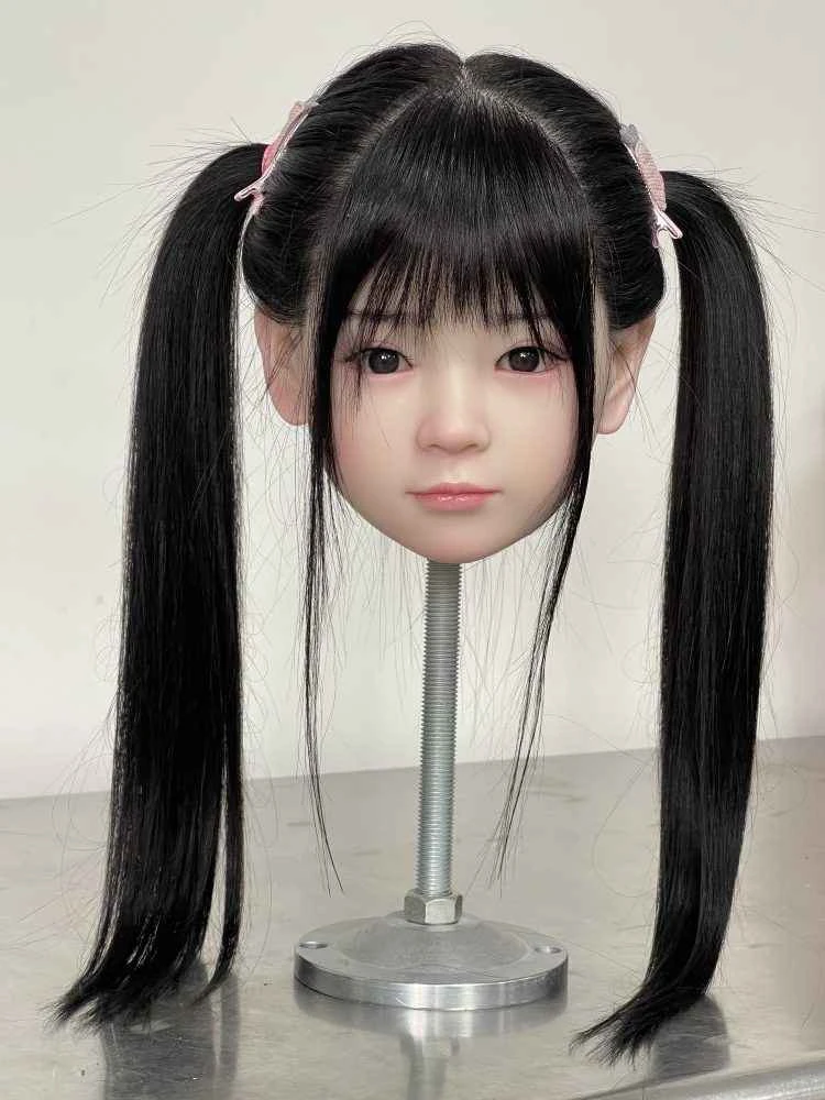
CATDOLL Cici Hard Silicone Head
Articles
2026-02-22

CATDOLL 88CM Q Full Silicone Doll
Articles
2026-02-22